Физика/7. Оптика
Yevtushenko D.A., Odarenko E.N.
Kharkiv National
University of Radioelectronics, Ukraine
V. N. Karazin Kharkiv National
University , Ukraine
Two-dimensional
photonic crystal structure with
nonlinear elements
Photonic technology, by use of light instead of relatively slow
electrons as the information carrier, is increasingly being proposed as a
replacement for electronics in communication and information management
systems.
Until recently, it was assumed that photonic crystals interact with
electromagnetic waves only through linear processes. This assumption was based
on the fact that the dielectric permittivity of materials does not depend on
the intensity of light. But, basically, the nonlinear effects can be observed
at high intensity of radiation.
Photonic crystals and their band gaps have opened a new chapter in
nonlinear optics. Photonic band gap is a frequency range where the propagation
of light is forbidden in all directions. The nonlinear optics of photonic
crystals, in fact, combines impressive achievements of laser physics and
ultrafast photonics with the possibilities of advanced modern technologies,
allowing one-, two-, and three-dimensional structures with a period of the
order of radiation wavelengths as well as photonic-crystal waveguides,
resonators, fibers and membranes to be fabricated [1].
Photonic crystal structure with finite number of periods that arranged
on the nonlinear layer is considered in this work. Kerr nonlinearity is
assumed. The modeling of such structures and calculations of the dispersion diagrams
and transmittance are performed in software packages MEEP and MPB [2, 3].
We considered the photonic crystal structure that consists of infinity
dielectric cylinders. This system of cylinders located in the air. Elements
have radius equal to r = 0.35a where a is the period of structure.
The modeling structure is shown on Fig. 1 and it contains source of
radiation, detector for registration of the transmitted light, PML-layer around
the calculation domain and structure under investigation – photonic crystal with
nonlinear layer.
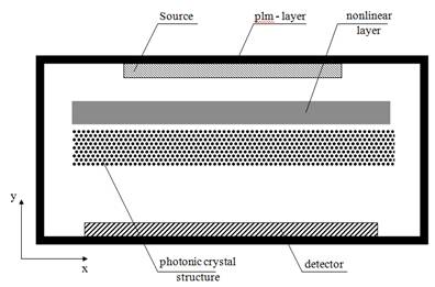
Fig. 1. Scheme of the structure for numerical calculation
Fig. 2 presents dispersion diagram of the dielectric photonic crystal. This diagram is calculated within the irreducible
Brillouin zone. The ordinate axis shows the normalized frequency. There are some band gaps which indicated by horizontal stripes. Fig. 3
shows the transmittance for this photonic crystal structure. It is clear that
forbidden zones on this figure are in good accordance with the dispersion
diagram (Fig. 2).
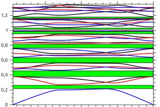
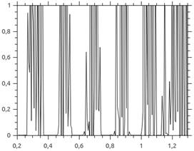
Fig. 3. Transmittance of the photonic crystal
|
|
Fig. 2. Dispersion diagram.
|
|
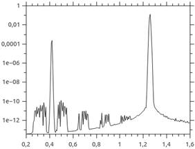
Fig. 4 shows the signal power in the detector area versus normalized
frequency. In this case wave at frequency 0.42 propagate through nonlinear layer.
We can see power peaks for 1st and 3rd harmonics. Photonic
crystal structure located on the nonlinear layer provides selection of the 3rd
harmonic of the signal (Fig. 5). Naturally, signal frequency (0.42) falls into
band gap of the photonic crystal and 3rd harmonic frequency (1.26)
is outside of any band gaps (Fig. 2 and 3).
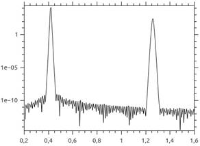
Therefore photonic crystal structure with Kerr nonlinear layer can be
used as frequency converter for laser radiation. Moreover under the certain
condition this system represents dual-frequency source of radiation when the
both harmonics propagate through the photonic crystal with approximately equal
amplitudes.
Литература:
1.
Joannopoulos
J.D., Meade R.D., Winn J.N. Photonic Crystals: Molding the Flow of Light. –
Princeton Univ. Press, 1995. – 137 p.
2.
Oskooi
A. F., Roundy D., Ibanescu M., Bermel P., Joannopoulos
J. D., Johnson S. G. MEEP: A
flexible free-software package for electromagnetic simulations by the FDTD
method // Computer Physics
Communications. – 2010.
– Vol. 181. – P. 687–702.
3. Johnson
S. G., Joannopoulos J. D. Block-iterative
frequency-domain methods for Maxwell's equations in a planewave
basis // Optics Express. – 2001, No 3. – pp. 173–190.