O.G.
Danalakiy, aspirant
National techical university
“ Kharkiv polytechnic institute”
Chernivtsi, Department
Ministry of Education, Ukraine.
Response
of a slot diode with a two-dimensional electron channel resonant terahertz
The
fundamental resonance behaves similar to the current resonance in a RLC
circuit. A conclusion is drawn that a slot diode with two-dimensional electron
chan-nel provides a resonant circuit at terahertz frequencies that couples
effectively to external electromagnetic radiation with loaded Q-factor
exceeding unity even at room temperature. The diode resistance may be measured
from contactless measu-rements of the characteristic electromagnetic lengths of
the diode. Terahertz respo-nse of a slot diode with two-dimensional electron
channel is calculated on the basis of the first principles of electromagnetism.
It is shown that all characteristic electro-magnetic lengths (scattering,
absorption and extinction lengths) as well as the impe-dance of the diode
exhibit resonances at the frequencies of plasmon excitation in the channel.
High-frequency response of field-effect transistors and diodes
with two-dimensional electron channels is strongly affected by plasma
oscillations in the channel. This phenomenon in its various manifestations can
be used for the detection, frequency multiplication and generation of terahertz
(THz) radiation [1-7]. One of the main parameters of a device,
which determines its high frequency properties, is the device impedance. The high-frequency impedance (admittance)
of a slot diode was calculated for capacitively [11] and conductively [12] contacted two-dimensional electron channel in the frame of the electrostatic
theory and an equivalent circuit approach. In these approaches, the radiative
contribution to the impedance (radiation resistance, Rrad, of the diode) is not accounted for and
inter-contact geometrical capacitance, Cg
, is either ignored altogether [11]
or treated as a free parameter [12].
1.Model theoretical. Consider a plane electromagnetic wave incident
normally from vacuum onto a perfectly conductive plane z = 0 with a slot of width w,
which is located on the surface of a dielectric substrate. We assume that the
electric field of the wave, ![]() , where
, where ![]() with c being the speed of light in
vacuum, is polarised across the slot (along
the x-axis). The edges of the slot are connected by a two-dimensional electron channel with the areal
conductivity described by the Drude model as
with c being the speed of light in
vacuum, is polarised across the slot (along
the x-axis). The edges of the slot are connected by a two-dimensional electron channel with the areal
conductivity described by the Drude model as
![]() ,
,
where ν is the electron momentum scattering
rate, N is the sheet electron
density, e and m* are the charge and effective mass of electron, respectively.
Our theoretical procedure involves the following
steps. We rewrite the Maxwell equations in the ambient medium and in the
substrate in the Fourier transform representation over the in-plane wave vector
kx . The Fourier
transforms of in-plane components of the electric and magnetic fields satisfy
the following boundary conditions at z = 0:
![]() ,
,
![]() ,
,
where j(kx ) is the Fourier transform of the surface electron current density, δ(kx )
is the Dirac, δ-function the subscripts a and s label the fields in
the ambient medium
and the substrate, respectively, and superscripts (ind) and (tot) refer
to induced and total fields, E0
and H0 are the amplitudes
of electric and magnetic fields in the incident wave. Then we relate the
Fourier transform of the surface electron current density in the diode plane to
that of the in-plane electric field in the same plane as
![]() ,
,
where ![]() is the Fourier transform of inplane component
of the total electric field in the diode plane, Z0 is the free-space impedance. The kx -space surface admittance G(kx ) depends exclusively on the frequency and dielectric
constants of the ambient medium, εa (which
we assume to be 1), and the substrate, εx :
is the Fourier transform of inplane component
of the total electric field in the diode plane, Z0 is the free-space impedance. The kx -space surface admittance G(kx ) depends exclusively on the frequency and dielectric
constants of the ambient medium, εa (which
we assume to be 1), and the substrate, εx :
![]() ,
,
where
 .
.
Coming back to the real-space representation we have
![]()
Using Ohm law j(x)= σ(ω)Ex(x) for
the two-dimensionalelectron channel and the condition Ex = 0 for the perfectly conductive contact semi-planes,
we arrive at the following integral equation for in-plane component of the
total electric field within the slot:
 (1)
(1)
with the kernel
![]() .
.
Integral equation (1) is solved numerically by the Galerkin method
through its projection on an orthogonal set of the Legendre polynomials within
the interval
[-w/2,w/2]. As a result we find the
induced electric field in the ambient medium as
![]() (2)
(2)
and the total electric field in the substrate as
![]() (3)
(3)
The electric fields ![]() and
and ![]() have zero y-components
and r is the
two-dimensional radius vector r={x,y}. The wave vectors ka(s) have kx and
have zero y-components
and r is the
two-dimensional radius vector r={x,y}. The wave vectors ka(s) have kx and ![]() as their components. The integrals in the right sides
of Eqs. (2) and (3) describe the scattered fields in terms of the planewave continuum, while the first summand in Eq. (2) is the wave reflected normally
from perfectly conductive plane. The sing before the radical in expression for
kz is chosen to correspond the
outgoing waves for
as their components. The integrals in the right sides
of Eqs. (2) and (3) describe the scattered fields in terms of the planewave continuum, while the first summand in Eq. (2) is the wave reflected normally
from perfectly conductive plane. The sing before the radical in expression for
kz is chosen to correspond the
outgoing waves for ![]() and evanescent waves for
and evanescent waves for ![]() is respective medium. Since only the outgoing plane
waves for
is respective medium. Since only the outgoing plane
waves for
![]() contribute to
radiative losses, we can calculate the fluxes of energy cattered per unit length of the slot in each
medium as
contribute to
radiative losses, we can calculate the fluxes of energy cattered per unit length of the slot in each
medium as
 ,
,
where na(s) is the internal normal to the
diode plane into respective medium. Then we can define the scattering length as
![]() in each medium, where P0 is the energy flux density in
incident wave. We can also introduce the total scattering length as
in each medium, where P0 is the energy flux density in
incident wave. We can also introduce the total scattering length as ![]() and the absorption length
and the absorption length ![]() , where
, where
is the energy absorption rate (per unit length of the slot).The
scattering and bsorption lengths obey the energy conservation law in the form ![]() , where
, where
 (4)
(4)
is the extinction length, which is the ratio between the amount of
energy picked out of the incident wave per unit time (per unit length of the slot) and the energy flux density in
incident wave. The formula analogous to Eq.
(4) is known as the optical theorem
in the scattering theory [10].
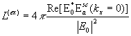
2. Results and ecsperement. Arrows
in Fig. 1 mark the frequencies of ungated
plasmons in isolated two-dimensional electron channel with wave vectors qn = (2n − 1) π/ω (n = 1; 2; 3;….),
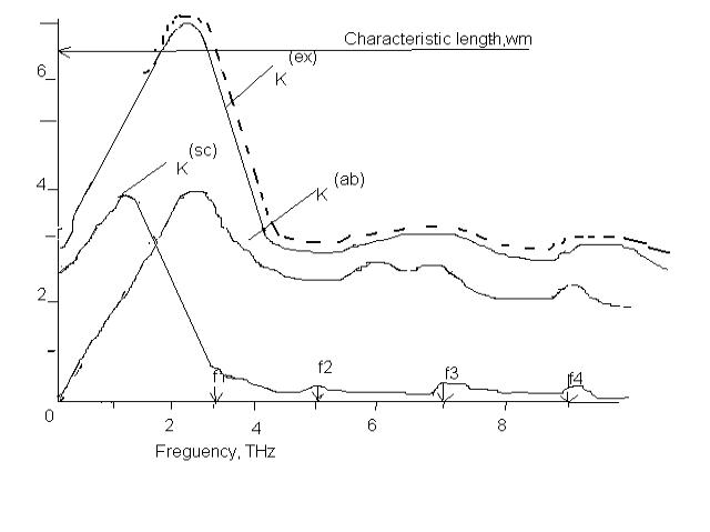
Figure 1. Characteristic lengths vs.
frequency for the slot diode with parameters: ![]() .
.
which are estimated by a simple approximate formula [11]:
 (5)
(5)
It is evident from Fig. 1 that the plasma oscillations in
the slot diode are softened because of
the induction of image charges in the perfectly conductive contact semi-planes
by plasma oscillations. In the equivalent circuit description, we can
haracterize the slot diode with two-dimensional electron channel
by its impedance. Within the channel the total current is the sum of the
electron current and displacement current caused by oscillating charges in both
the channel and contacts of the diode. Far away from the slot, the current in
the contact planes is purely conductive and is determined by the amplitute of
incident wave.
Since the total current is conserved along
the circuit, we can define the diode impedance Z = R + iX (per unit length
of the slot) as
where I = 2E0/Z0 is the surface current density induced by the
incident wave in the perfectly conductive contact planes. The frequency
dependence of the diode normalized impedance shown in Fig. 2 displays resonances at the plasmon excitation frequencies.
The
reactance, X, exhibits transition
from inductive (X < 0) behavior
caused by the kinetic inductance of the electron channel to a capacitive behavior
(X > 0) at the frequency of the fundamental plasmon
resonance, which corresponds to the current resonance in the equivalent circuit
description. However, no current resonance is exhibited at higher plasmon
resonant frequencies.
The normalized
resistance, R/Z0, is, in essence, the matched width of the diode
(measured along the slot), since the resistance of diode with the matched width
is equal to the free-space impedance. The following theorem is valid: 4R = Z0L(ex).
The extinction length calculated using this formula (dashed curve in Fig. 1) and by Eq.
(4) (solid line)coincide within the accuracy of our numerical procedure. Accordingly,
we can introduce the electron resistance, Re, and radiation resistance, Rrad, where Re = Z0L(ab)/4 and Rrad = Z0L(sc)/4, respectively, so that the
total resistance of the diode is given by R
= Re + Rrad. Note that R does not vanish
at high frequencies (but approaches Rrad
instead).
One can see from
Fig. 2 that higher resonances are not
nearly so pronounced as predicted by the electrostatic description [12] because RradCg
circuit effectively shunts plasma oscillations in the channel at high frequencies.
However, a sharp
fundamental resonance, which corresponds to the current resonance in the
equivalent circuit description, shows up even for room temperature parameters
of the diode. The frequency of the fundamental plasma resonance in the slot
diode increases with decreasing the slot width (according to formula (5) it
varies roughly as a square root from the inverse of the slot width).
Figs. 3 and 4 exhibit absorption length and scattering length
spectra for 100-nm width of the slot for different electron scattering rates.
Notice that the resonant absorption (the excess of the absorption at the
resonance over the non-resonant Drude background) grows considerably with
decreasing the width of the slot (cf.
Figs. 1 and 3). Clearly, the
fundamental plasma resonance becomes narrower with decreasing the electron
scattering rate. However, the width of the resonance remains finite due to the radiative
damping
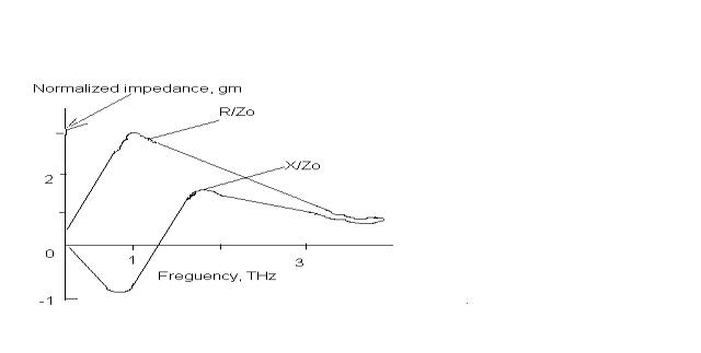
Figure 2. Impedance of the slot diode with
two-dimensional electron channel vs. frequency.
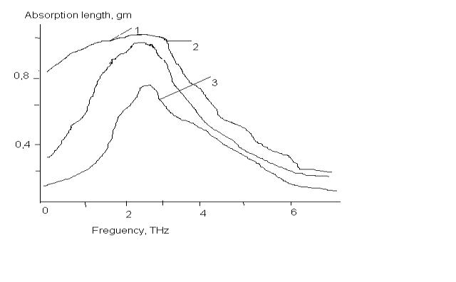
Figure 3. Absorption length of the slot
diode with parameters: ![]() as a function of the
frequency for different electron scattering rates:
as a function of the
frequency for different electron scattering rates: ![]() (curve 1);
(curve 1); ![]() (curve 2);
(curve 2); ![]() (curve 3).
(curve 3).
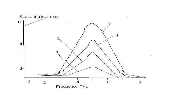
Figure 4. Scattering length of the slot
diode as a function of the frequency for different electron scattering rates ![]() (curve 1);
(curve 1); ![]() (curve 2);
(curve 2); ![]() (curve 3)
(curve 3) ![]() (curve 4).Other parameters of the diode are
the same as those in Fig. 3.
(curve 4).Other parameters of the diode are
the same as those in Fig. 3.
Оf plasma oscillations
even with no electron scattering in the channel. The width of the scattering
resonance in the absence of electron scattering (see curve 4 in Fig. 4) is entirely of the radiative damping
origin.To minimize an error arisen from the
non-resonant background contribution, we estimate the radiative damping of
plasmons, rad, as the half width at half magnitude (HWHM) in the low-frequency slope of the scattering resonance curve for ![]() (curve 4
in Fig. 4), which yields
(curve 4
in Fig. 4), which yields ![]() . Then the electron scattering contribution to the resonance linewidth can be obtained as a
difference between the (HWHM) measured in the low-frequency slope of the scattering resonance
at any given ν ≠ 0 (or, which yields the same result, in the high-frequency slope of the
corresponding absorption resonance) and
the radiative damping.
. Then the electron scattering contribution to the resonance linewidth can be obtained as a
difference between the (HWHM) measured in the low-frequency slope of the scattering resonance
at any given ν ≠ 0 (or, which yields the same result, in the high-frequency slope of the
corresponding absorption resonance) and
the radiative damping.
The scattering
length at the plasma resonance monotonically grows with decreasing the electron
scattering rate, while the resonant absorption
exhibits maximum when the dissipative broadening (caused by the electron
scattering in the channel) of the resonance linewidth becomes equal to the radiative broadening (curve 2 in Fig. 3 corresponds
to this case).
Both the weaker as well as stronger electron scattering
result in smaller resonant absorption. Note that under the condition of maximal absorption the
scattering length of the diode is approximately equal to its absorption length,
which puts the limit of the absorption-to-scattering length ratio of the diode
close to unity.
We conclude that a slot diode with two-dimensional electron
channel provides a resonant circuit at terahertz frequencies that effectively couples to external
electromagnetic radiation with the loaded Q-factor
exceeding unity even at room temperature. We also claim that the diode high-frequency
resistance may be measured from contactless measurements of the chatacteristic
electromagnetic lengths of the diode.
References
[1] D. G. Bernik, H.U. Verdov.
In.: Terahertz Sources and Systems, ed.by R. Miles,
S. Harrisson
and F. Lippens (Dordrecht, Kluwer, 2007) p. 158.
[2] R. K.
Saraton, M. D.Nacrjd. Phys. Rev. Lett., 74, 248 (2008).
[3] U. L. Bortyiy, E.M. Mark. IEEE
Trans. Electron. Dev., 54, 203 (2008).
[4] M.S.Vzrahl, IEEE Trans. Microwave Theory and Techniques, 57, 680 (2007).
[5] F.
G.Amoahii, S.V. Kachovskii, G.K. Simin, X. Nu, M. Asif Khan, S.A. Saylor,
L.C. Brunel. J. Appl. Phys., 95, 457
(2006).
[6] U.
L. Bortyiy, Y. Deng, M. D.Nacrjd. Appl. Phys. Lett., 54, 7294 (2006).
[7] U.V. Eisenstein. Appl. Phys. Lett., 86, 146
(2008). Resonant terahertz response
of a slot diode with a two-dimensional electron 248.
[8] O.G.
Danalakiy, M.R. Natozki, S.L. Volcov,. Phys. Solid
State, 65, 204
(2008).
[9] F.
G.Amoahii, R. Kersting, O.G.
Danalakiy.
Appl. Phys. Lett., 88, 27 (2008).
[10] A.V. Antonov,
V.I. Gavrilenko, A.O.Kuhir.
Phys. Solid State, 41, 617 (2006).
[11] U. L.
Bortyiy, P.Q.
Verdov. Appl. Phys. Lett., 345, 263 (2008).
[12] V. Ryzhii, F. G.Amoahii, R.
K. Saraton. Phys., 67, 208 (2007).