Физика/2.Физика твердого тела.
Svetlana A.
Barannikova1,2, Galina V. Shlyakhova1,3, Lev
B. Zuev1,2
1Institute of
Strength Physics & Materials Science, SB RAS, Tomsk, Russia
2National
Research Tomsk State University, Tomsk, Russia
3Seversk
Technological Institute affiliated to NIYaU MIFI, Seversk, Russia
Investigation
of the Localized Plastic Deformation Zone of Superconducting Cable
Using atomic
force and optical microscopy methods, the changes in the
microstructure within the localized plastic deformation zone were investigated for the alloy Nb47%Ti used
for the manufacture of superconducting cable employed as current-carrying
elements in the International Thermonuclear Experimental Reactor [1,2].
Several layers of material 0.5-mm each were removed with the aid of abrasive
from the latter zone to be examined by metallography technique. It was found
that all the Nb-Ti strands of the inner layer adjacent to the copper core have
a round shape. The treatment by cold drawing has left traces in the intermediate
layer of the region adjacent to the copper core. The Nb-Ti strands in the outer
layer are rhomb-shaped. The cross-section topography was examined by the
methods of optical and atomic-force microscopy. After the region adjacent to
the copper core had been polished with abrasive to a depth of 0.5 mm, Nb-Ti
strands on its border would assume irregular shape and would form a localized
deformation zone similar to that observed for as-received Nb-Ti strands which
have not been polished (Fig. 1 a, b). In the point of rupture the
intermediate copper matrix layer separating Nb-Ti strands had average grain
size ~850 nm. The statistic treatment data suggests that the average grain size
of the defect-free zone of the copper matrix has average grain size ~800 nm,
which is comparable to that of copper in the point of rupture, i.e. ~850 nm [1].
The profilogram obtained for the cross-section polished to a depth of 0.5 mm
shows a Nb barrier in the point of rupture, which surrounds Nb-Ti strands
within the copper matrix. This presents a series of high-amplitude sharp maxima
having width ~250 nm, which is similar to that observed for as-received
material without polishing. A similar Nb barrier surrounding Nb-Ti strands in
the location of breakage was observed for material that had been polished to a
depth of 1 mm.
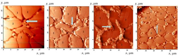 (a)
(b) (c) (d)
(a)
(b) (c) (d)
Fig. 1 The AFM image of the zone of
localized plastic deformation at the point of breakage of Nb-Ti strands
(designated by arrows): 1–copper matrix; 2–Nb-Ti strands; depth of polishing: (a) 0 mm; (b) 0.5 mm; (c) 1 mm; (d) 2 mm
Metallography investigation was performed
for Nb-Ti strands cross-sections, which were subjected to etching and polishing
to a depth of 1 mm. It was found that Nb-Ti strands appear to be unchanged by
comparison with as-received unpolished material. However, the localization zone
has a different aspect (Fig. 1 c).
The lobe-like strands coalesce to form one strand, which suggests that the
strands are of different thickness. The Nb-Ti strands within the localization
zone assume a round shape. The structure of section surface, which had been
polished to a depth of 2mm, was examined in an optical microscope. The general
aspect of localization zone is found to have changed significantly relative to
as-received defect-free state. The Nb-Ti strands in the point of rupture
gradually form a conglomerate (Fig. 1 d);
the near-lying Nb-Ti strands have a round shape, which is characteristic for defect-free
zones. It should be noted that another defect was found to occur in the
vicinity of boundary between the intermediate layer of Nb-Ti strands within the
copper matrix and the copper core, i.e. two Nb-Ti strands of irregular shape,
which had smaller size relative to the near-lying ones. Using the contact
method of AFM technique, we examined the cross-section surface of Nb-Ti strands
which had been subjected to etching an polishing to a depth of 2 mm. In this
case, a Nb barrier is found to occur on both the inner and the outer surface of
the Nb-Ti strands in copper matrix. As noted above, a similar Nb barrier had
been observed previously in a defect-free area of as-received material; this
shows in profilograms as a series of high-amplitude narrow maxima having width
≤ 250 nm. The evolution of localized plasticity zone is illustrated in
Figs. 1. Thus, the area next to the cable copper core is found to contain
localized deformation zone in the point of rupture of Nb-Ti strands. Moreover,
the Nb barrier is present only partially in the same area, which is indicative
of a varying extent of deformation in the sections, which were polished to
depths varying from 0.5, 1 and 2 mm. A major drawback to the conventional
approach employed in the analysis of the ultimate
tensile strength of superconductors on the base of Nb-Ti alloy is the
conceptual representation of plastic deformation as a steady-state and
homogeneous process. The experimental evidence for the nature of plastic
deformation strongly suggests that at the early stages of straining the plastic
deformation would exhibit an inhomogeneous behavior, which is liable to cause
formation of localized plasticity nuclei [3]; in one of these nuclei rupture of
cable strands would occur. The macro-scale localization of deformation has been
studied in sufficient detail [3].
The work was performed in the
frame of the Tomsk State University Academic D.I. Mendeleev Fund Program and
the Program of Fundamental Research of State Academies of Sciences for the
period 2013-2020 yrs.
References
1. L.B. Zuev, G.V. Shlyakhova, S.A.Barannikova, S.V. Kolosov,
Microstructure of elements of a superconducting alloy Nb-Ti cable, Russ. Metal.
2013 (2013) 229-234.
2. G.V. Shlyakhova, S.A. Barannikova, L.B. Zuev,
On structure of localization zones of plastic
deformation in superconductive cable based on Nb-Ti alloy, Metallofiz. Nov. Tekhnol. 35 (2013) 453 – 465.
3. L.B. Zuev, V.I. Danilov, S.A. Barannikova, V.V. Gorbatenko, Autowave
model of localized plastic flow of solids, Phys. Wav. Phen. 17 (2009) 1–10.