D. Yermukhamed
al-Farabi Kazakh National University, Almaty,
Kazakhstan
Formation of the thin layers of
organometal perovskites by vacuum evaporation method for application in solar
cells
Nowadays the subject of attention
from specialists in the field of solar energy become materials, which called
perovskites. During the short time we obtained solar cells with coefficient of
performance (COP) of 3.8% in 2009 to 20.29% in 2015. World began to talk about
the remarkable success of CH3NH3PbX3 organometallic
threehalogen perovskites (where X - I, Br, Cl halogens, or their mixtures), and
about perovskite photovoltaics era. With this material began to have great
expectations for the development of highly efficient solar cells with cost much
lower (4-6 times) than cost of elements based on crystalline silicon, which is
basic material of modern photovoltaics.
It should be noted that the creation
of perovskite solar cells was observed by «Science» journal, as one of the
technical achievements of 2013. Perovskite solar cells manufacturing do not
require expensive clean rooms and technological equipment, and materials.
Formation of perovskite material required temperature that do not exceeding 150
° C.
In this article represented results
on the formation of perovskite layers by different vapor phase methods. In
vapor phase method organic part is treated by vapour of inorganic part; it is a
method of perovskite layers formation with wide band gap, which provides method
of producing CH3NH3PbBr3 wide-perovskite. This
perovskite may be used to create cascade solar cells, as frontal heterojunction element.
In this experimental work used vacuum evaporation methods such as vapor
deposition with dual source and deposition by vapour assisted solution process
to produce organometallic perovskites.
During vapor deposition with double source, we put in separate crucibles
500 mg CH3NH3I and 100 mg PbCl2. Substrate
fixed on substrate holder, which disposed above sources with FTO coated TiO2
converted down to the sources. After evacuating of pressure in chamber to 10-5 mbar, two sources were
heated slightly above the desired deposition temperature for 5 minutes (CH3NH3I
heated to 120 ° C, and PbCl2 to 325 ° C) to remove volatile
impurities before material deposition on substrate. The substrate holder
rotated for uniform deposition of coating, because the right source
predominantly covers the right side of substrate, which is similar to the left
source. The substrate holder cooled by water at about 21 ° C, although the
precise measurement of substrate temperature during the deposition process was
not carried out.
In Figure 1 schematically illustrated system of deposition with dual
source.
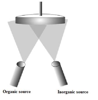
Figure 1 - Schematic image of
deposition system of materials. Thermal evaporation system with dual source for
deposition of perovskite absorber; organic source - methylammonium iodide and
inorganic source - lead chloride
Perovskite films have been optimized for improved device performance [1]
by applying the changes in key parameters such as speed and deposition time for
two sources. In particular, the performance of device [2] is very dependent on
the ratio of CH3NH3I to PbCl2 content, and the
total deposition thickness.
Perovskite films obtained by vapor deposition with dual source were
homogeneous [3]. Vapor deposition can lead to fully optimize the electronic
contact on the borders through
plurality of layers with controlled doping levels.
The following method which was used for manufacturing the organic /
inorganic hybrid perovskite films – is a deposition by vapour assisted solution
process. In this method, inorganic film structures is formed by depositing
precursor solution onto substrate, followed by treatment with vapors of
necessary organic compounds [4]. PbI2 and CH3NH3I
- corresponding vapours of precursors that form CH3NH3PbI3.
PbI2 films deposited on the FTO glass coated by compact and
mesoporous TiO2 layer, followed by annealing in CH3NH3
vapour at 150 ° C under nitrogen atmosphere for 2 hours to form perovskite
films (CH3NH3PbI3).
In Figure 2 represented schematic image of perovskite film forming by
vapour assisted solution process.
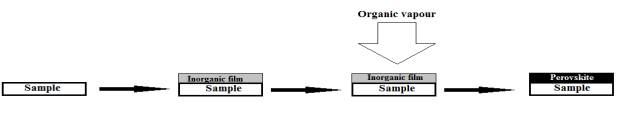
Figure 2 - Schematic image of the
formation of perovskite film with vapour assisted solution process
Vapour assisted solution process method is a low-temperature method for
production of perovskite films based on kinetically favorable reactions between
the newly deposited PbI2 film and CH3NH3I
vapour [5].
A key step in this method is the growth of film during the direct
reaction of just deposited PbI2 film with CH3NH3I
vapor phase. It uses kinetic reactivity of CH3NH3I and
thermodynamic stability of perovskite during the immediate growth of film; in
the result produced films with well
defined grain structure with grain size of several microns, with complete coverage
of the surface and small surface roughness of surface suitable for photovoltaic
applications.
In Figure 3 shown SEM images of films surface prepared from the solution
and by vapor-phase method. The films deposited from vapor is extremely
homogeneous. In contrast, the films treated in the solution, covered partially
the substrate with crystalline islands on tens of micrometers of scale length.
Voids between crystals in the film treated in solution apparently reach
directly glass coated by compact TiO2 and FTO. Perovskite film,
deposited from vapour, is uniform and similar to the FTO layer with a little
more crystallinity in appearance. Perovskite film obtained from solution, has
an extremely smooth surface, in accordance with the larger size of crystalline
particles.
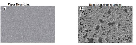
Figure 3 - Characteristics of the
topology of thin films. SEM images of the surface (a) perovskite films
deposited from vapour and (b) perovskite film treated in the solution
Perovskite film obtained by deposition by vapour assisted solution
process method have full coverage of the surface, uniform grain structure with
a grain size of more than micron and
100% conversion of the precursor. Rebuilding of PbI2 film during the
implementation of CH3NH3I conditioned by decreasing
energy of grain boundaries. Vapour assisted solution process method is simple,
manageable and universal method in an effort to achieve high quality of
perovskite films, and therefore, photovoltaic devices with high efficiency. The
inclusion of organic compounds in the deposited inorganic structures by vapour
effectively prevents from a high rate of reaction (formation) of perovskite
during coprecipitate precursor, and also eliminates the possibility of film
deterioration which sometimes observed during the immersion of inorganic
structure to solution with organic compounds.
The roughness of film produced by vapour assisted solution process
method is small. The resulting film has thickness of about 350 nm, with
distinct grains across the whole thickness of film. 100% surface coverage,
microscale grain size and uniform grain structure make this prepared film
promising to use in photovoltaic devices. These characteristics may be
associated with relative smoothness of PbI2 films.
1. Were carried out research works on the formation of perovskite films
by vapor deposition methods with a dual source and deposition by vapour
assisted solution process.
2. We used three-layer version of the front contact consisting of FTO
layers, blocking and mesoporous TiO2 layers. Blocking TiO2
layer prevents entering of holes to the FTO. Photoconverters based on
mesoporous have several advantages over the planar devices such as higher
efficiency, less hysteresis effect.
3. Using the methods of scanning microscopy were
studied structural properties and determined the thickness of perovskite layer.
In work was found optimal deposition regimes, under which formed perovskite
thin layers.
4. Considering methods show that can get
organometallic perovskites films with high-quality for further practical
application in solar cells and lasers. Another advantage of metal halide
perovskite lasers is their frequency tuning in the visible range. This can be
easily achieved through the replacement of iodide ions by bromide.
5. Based on the experimental data one can conclude
that the obtained films is not inferior to known literature methods and are
suitable for use in photovoltaic devices.
Literature:
1.
Lee,
M. M., Teuscher, J., Miyasaka, T., Murakami, T. N. & Snaith, H. J.
Efficient hybrid solar cells based on meso-superstructured organometal halide
perovskites. Science 338,643–647 (2012).
2.
Ball,
J. M., Lee, M. M., Hey, A. & Snaith, H. J. Low-temperature processed
meso-superstructured to thin-film perovskite solar cells. Energy Environ. Sci.
6, 1739–1743 (2013).
3.
Liu M., Johnston M. B., Snaith H. J. Efficient planar
heterojunction perovskite solar cells by vapour deposition //Nature. – 2013. –
Vol. 501. – №. 7467. – P. 395-398.
4.
Chen
Q. et al. Planar heterojunction perovskite solar cells via vapor-assisted
solution process //Journal of the American Chemical Society. – 2013. – Vol.
136. – №. 2. – P. 622-625.
5.
K.
Liang, D. B. Mitzi and M. T. Prikas, Synthesis and Characterization of
Organic-Inorganic Perovskite Thin Films Prepared Using a Versatile Two-Step
Dipping Technique, Chem. Mater., 1998, 10, 403–411.
Резюме
В этой работе рассматривается получение пленок перовскита
с помощью методов вакуумного
испарения. А именно
методами, парофазного осаждения с двойным источником и осаждения обработкой из раствора индуцированное паром.
Были
определены преимущества и
недостатки данных экспериментальных методов. Были исследованы структурные
свойства пленок с помощью
сканирующего электронного микроскопа. Были
найдены оптимальные режимы осаждения тонких слоев перовскита.
Ключевые слова:
органометаллический перовскит, парофазное осаждения с двойным источником, осаждение обработкой из раствора
индуцированное паром, СЭМ изображение.